- 您现在的位置:买卖IC网 > Sheet目录323 > EFM32G-DK3550 (Energy Micro)KIT DEVELOPMENT EFM32 GECKO
�� �
�
�...the� world's� most� energy� friendly� microcontrollers�
�?�
�?�
�?�
�?�
�Support� for� offset� and� gain� calibration�
�Output� to� ADC�
�Sine� generation� mode�
�Optional� high� strength� line� driver�
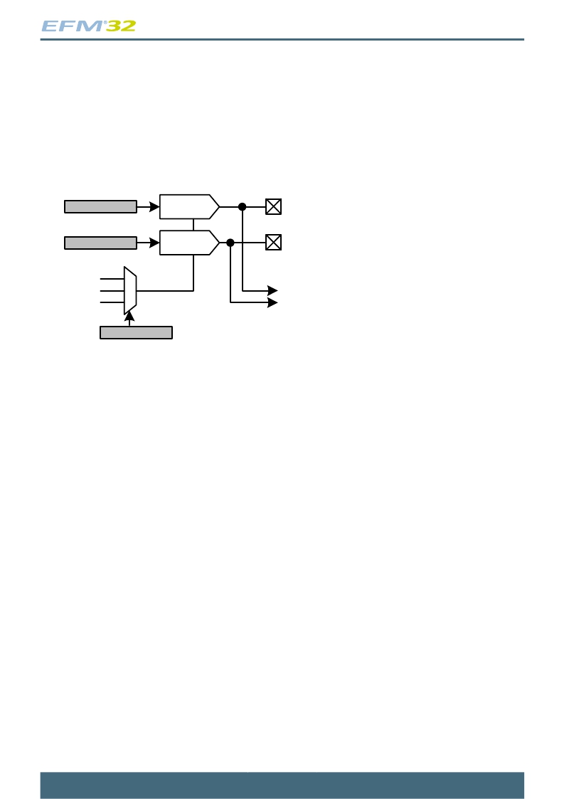
�26.3� Functional� Description�
��Figure� 26.1.� DAC� Overview�
�CH0DATA�
�CH1DATA�
�1.25� V�
�2.5� V�
�VDD�
�Ch 0�
�Ch 1�
�DACn_OUT0�
�DACn_OUT1�
�ADC�
�REFSEL�
�26.3.1� Conversions�
�The� DAC� consists� of� two� channels� (Channel� 0� and� 1)� with� separate� 12-bit� data� registers�
�(DACn_CH0DATA� and� DACn_CH1DATA).� These� can� be� used� to� produce� two� independent� single� ended�
�outputs� or� the� channel� 0� register� can� be� used� to� drive� both� outputs� in� differential� mode.� The� DAC� supports�
�three� conversion� modes,� continuous,� sample/hold,� sample/off.�
�26.3.1.1� Continuous� Mode�
�In� continuous� mode� the� DAC� channels� will� drive� their� outputs� continuously� with� the� data� in� the�
�DACn_CHxDATA� registers.� This� mode� will� maintain� the� output� voltage� and� refresh� is� therefore� not�
�needed.�
�26.3.1.2� Sample/Hold� Mode�
�In� sample/hold� mode,� the� DAC� cores� converts� data� on� a� triggered� conversion� and� then� holds� the� output�
�in� a� sample/hold� element.� When� not� converting,� the� DAC� cores� are� turned� off� between� samples,� which�
�reduces� the� power� consumption.� Because� of� output� voltage� drift� the� sample/hold� element� will� only� hold�
�the� output� for� a� certain� period� without� a� refresh� conversion.� The� reader� is� referred� to� the� electrical�
�characteristics� for� the� details� on� the� voltage� drift.�
�26.3.1.3� Sample/Off� Mode�
�In� sample/off� mode� the� DAC� and� the� sample/hold� element� is� turned� completely� off� between� samples,�
�tristating� the� DAC� output.� This� requires� the� DAC� output� voltage� to� be� held� externally.� The� references�
�are� also� turned� off� between� samples,� which� means� that� a� new� warm-up� period� is� needed� before� each�
�conversion.�
�26.3.1.4� Conversion� Start�
�The� DAC� channel� must� be� enabled� before� it� can� be� used.� When� the� channel� is� enabled,� a� conversion�
�can� be� started� by� writing� to� the� DACn_CHxDATA� register.� These� data� registers� are� also� mapped� into�
�2011-04-12� -� d0001_Rev1.10�
�366�
�www.energymicro.com�
�发布紧急采购,3分钟左右您将得到回复。
相关PDF资料
EFM32GG-STK3700
KIT STARTER GIANT GECKO
EFM32LG-DK3650
KIT DEV EFM32 LEOPARD GECKO
EK-K7-KC705-CES-G-J
KINTEX-7 FPGA KC705 EVAL KIT
EK-S6-SP601-G
KIT EVAL SPARTAN 6 SP601
EK-S6-SP605-G
KIT EVAL SPARTAN 6 SP605
EK-V6-ML631-G-J
VIRTEX-6 HXT FPGA ML631 EVAL KIT
EK-V7-VC707-CES-G
VIRTEX-7 VC707 EVAL KIT
EK-Z7-ZC702-CES-G
ZYNQ-7000 EPP ZC702 EVAL KIT
相关代理商/技术参数
EFM32GG230F1024
功能描述:ARM微控制器 - MCU 1024KB FL 128KB RAM
RoHS:否 制造商:STMicroelectronics 核心:ARM Cortex M4F 处理器系列:STM32F373xx 数据总线宽度:32 bit 最大时钟频率:72 MHz 程序存储器大小:256 KB 数据 RAM 大小:32 KB 片上 ADC:Yes 工作电源电压:1.65 V to 3.6 V, 2 V to 3.6 V, 2.2 V to 3.6 V 工作温度范围:- 40 C to + 85 C 封装 / 箱体:LQFP-48 安装风格:SMD/SMT
EFM32GG230F1024G-E-QFN64R
功能描述:IC MCU 32BIT 1MB FLASH 64QFN 制造商:silicon labs 系列:Giant Gecko 包装:剪切带(CT) 零件状态:在售 核心处理器:ARM? Cortex?-M3 核心尺寸:32-位 速度:48MHz 连接性:I2C,IrDA,智能卡,SPI,UART/USART 外设:欠压检测/复位,DMA,POR,PWM,WDT I/O 数:56 程序存储容量:1MB(1M x 8) 程序存储器类型:闪存 EEPROM 容量:- RAM 容量:128K x 8 电压 - 电源(Vcc/Vdd):1.98 V ~ 3.8 V 数据转换器:A/D 8x12b,D/A 2x12b 振荡器类型:内部 工作温度:-40°C ~ 85°C(TA) 封装/外壳:64-VFQFN 裸露焊盘 供应商器件封装:64-QFN(9x9) 标准包装:1
EFM32GG230F1024-QFN64
制造商:Energy Micro AS 功能描述:GIANT GECKO MCU - Cut TR (SOS) 制造商:Energy Micro 功能描述:GIANT GECKO MCU 制造商:Energy Micro AS 功能描述:IC MCU 32BIT 1MB FLASH 64QFN
EFM32GG230F1024-QFN64T
制造商:Energy Micro AS 功能描述:GIANT GECKO MCU - Trays
EFM32GG230F1024-QFN64-T
制造商:Energy Micro AS 功能描述:IC MCU 32BIT 1MB FLASH 64QFN
EFM32-GG230F1024-SK
制造商:Energy Micro AS 功能描述:GIANT GECKO SAMPLE KIT - Bulk
EFM32GG230F1024-T
制造商:Energy Micro AS 功能描述:IC MCU 32BIT 1MB FLASH 64QFN
EFM32GG230F512
功能描述:ARM微控制器 - MCU 512KB FL 128KB RAM
RoHS:否 制造商:STMicroelectronics 核心:ARM Cortex M4F 处理器系列:STM32F373xx 数据总线宽度:32 bit 最大时钟频率:72 MHz 程序存储器大小:256 KB 数据 RAM 大小:32 KB 片上 ADC:Yes 工作电源电压:1.65 V to 3.6 V, 2 V to 3.6 V, 2.2 V to 3.6 V 工作温度范围:- 40 C to + 85 C 封装 / 箱体:LQFP-48 安装风格:SMD/SMT